SEMI Standard – EDA(Equipment Data Acquisition) (or Interface A)
1. The change of Semiconductor processing and manufacturing technology
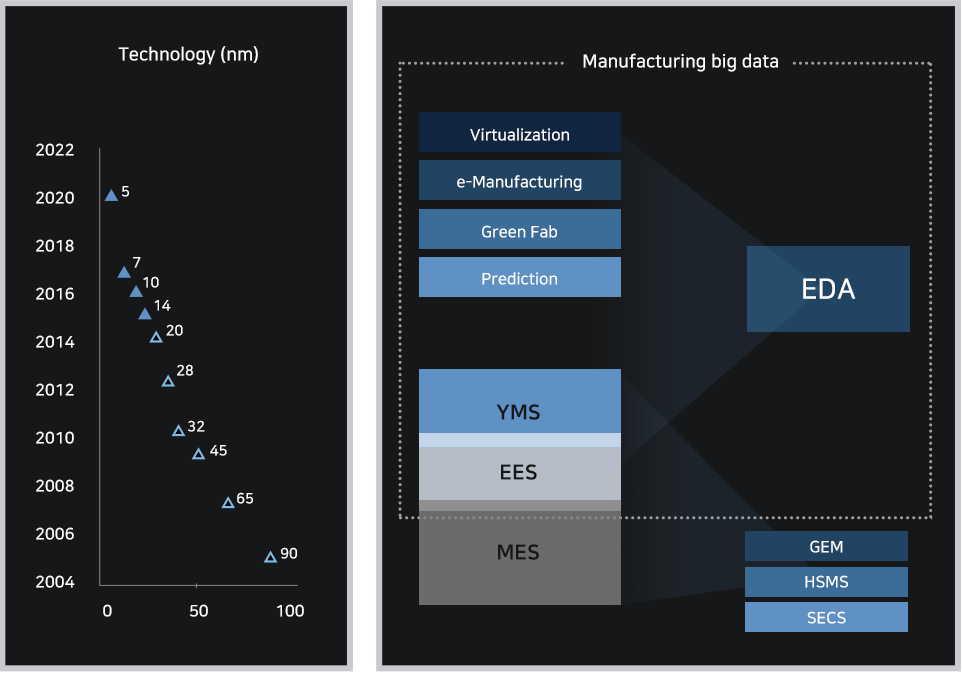
1) The increase in demand of collecting fine processing data by development of semiconductor processing technology.
/ Trend of Fine Processing Development |
KrF(248nm), ArF(193nm) > F2(157nm), Ar2(126nm) > EUV(13.5nm)Litho > DubblePatterning(DPT) > QuadruplePatterning(QPT)Nand Flash structure > 2D, 3D FinFET structure |
/ The increase in demand of collecting data by development of fine processing data
: Necessity of High resolution data under 0.1 sec. by the increase of fine process section
/ The extension of TAT by the increase of process step
: The increase in demand of collecting and analyzing data for the productivity improvement and the decrease of defect rate
2) The direction of manufacturing technology by the development of process technology

2. The technology background and necessity of EDA Standard
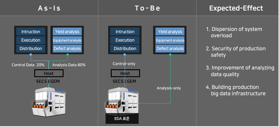
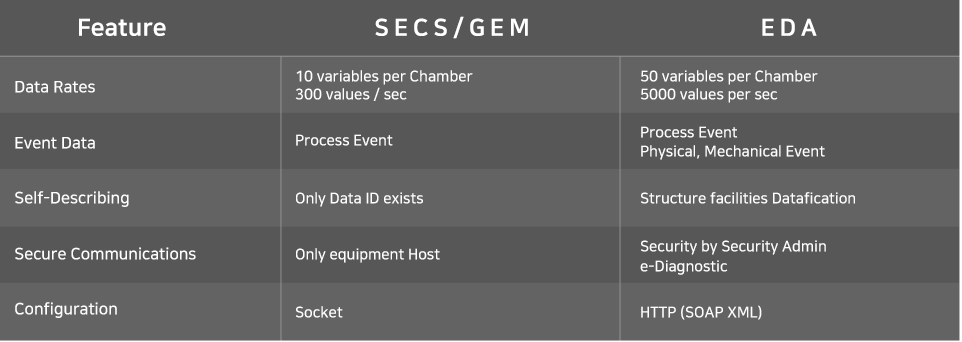
/ According to evolution of process technology, much more Sensor Parameter and Equipment Event Data are demanded to analyze equipment capacity, transference number and productivity. (more than about 80% of the entire data)
/ SECS(Semiconductor Equipment Communication Standard) was established in 1982 mainly for the equipment control and the operation of factory system.
/ SEMI established analysis-only protocol to overcome the limitations of SECS communication Channel and to meet the demand for data analysis. It is called EDA(Equipment Data Acquisition) Standard.
3. The Merit and Effect of SEMI EDA Standard
 |
Separation SECS Data Channel & Multi-Session
|
 |
Stabilizing production system by the independent Channel
|
 |
Supporting Data Collection Manager
|
4. EDA(Interface A) technology effect
1) The supply of Semiconductor next generation communication EDA solution
. Providing production and quality Big Data analysis base by collecting equipment fine data (10Hz↓(1Hz))
. Secure leadership of international standard
. International competitiveness reinforcement of semiconductor and equipment companies
2) Collecting data , modeling, developing control / management solution
. Build production automation base using semiconductor communication standard
. Improve small and medium manufacturing company’s production Process and realize System Base Manufacturing
5. EDA(Interface A) ?
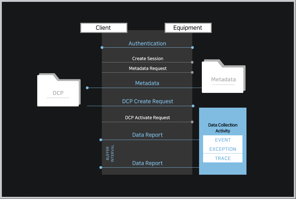
WSDLs and XML schemas based on SOAP XML is defined as SEMI Standard
EDA is consist of 4 parts that offer service for collecting equipment data.

6. EDA(Interface A) Scenario Overview
